- Admissions
- Academics
- Research Office
- Student Life
- News & Events
- Outreach
- About
Dr. Sufian Abedrabbo is currently an Associate Professor of Physics. Before Joining KU, Dr. Abedrabbo served in the University of Jordan, New Jersey Institute of Technology, Stevens Tech and Rutgers University. He also worked as an advisor to the CEO of the Jordan Investment Board on investments related to Semiconductors and Communications from 2006-2009. He has earned his PhD in Applied Physics in 1998 from the federated Applied Physics program of the New Jersey Institute of Technology (NJIT) and Rutgers the State University of New Jersey, specializing in Semiconductor Processing and Process Monitoring. He has over 27 years of experience in Silicon processing that includes Si-LED candidates, Si-photovoltaic and Si-Micro-electro-mechanical sensors. His other interests are optical components that include active impurity centers (Rare-Earth-Metals), sol-gel processes for synthesizing ceramic nanocomsposite candidates for energy storage, Si-anode structures for lithium ion batteries and engineering interfacial strains by interfacing silicon with various dielectrics to tailor the bandgap.
High Efficiency Bandgap Radiation from Silicon Interfaced with Sol-Gel Films
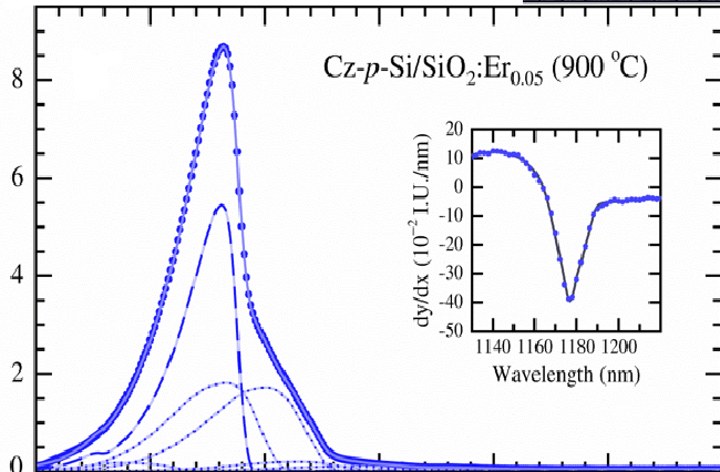
This project investigates photonic structures with novel functions fabricated by interfacing sol-gel films with crystalline silicon surfaces. Preliminary results using erbium-doped films show that this combination yields high emission levels for band-gap radiation from the silicon has disclosed an unexpected property of photonic materials. This is significant for surmounting obstacles to emission posed by the indirect band gap nature of crystalline Si, where free carriers usually recombine non-radiative generating heat rather than photons.
The experimental approach is to use test structures processed on Si and silicon-on-insulator (SOI) material for improved optical and electronic isolation and resolution. Experimental techniques for studying relevant aspects of the materials and photonics science are specifically: excitation-matrix photoluminescence, lifetime measurements, emission depth profiling, strain measurement by X-ray diffraction and micro-Raman spectroscopy, infrared spectroscopy, MOS capacitor analysis, and electrical transport.
Research goals are characterizing the optically active region in the silicon, indicated to lie adjacent to the interface with the sol-gel film, and quantifying internal and external emission quantum efficiencies. Relating film composition and mechanics to optical modifications of the adjacent silicon will also be fully explored.

Achieving Enhanced Radiative Properties for Indirect Bandgap Semiconductors by Surface Modifications via Ion Implantation and Ion-Beam Mixing
This project investigates surface modifications by ion implantation and ion-beam mixing of Si and other dopants including same group species (e.g. Si in Si or Ge in Si) seeking enhanced radiative properties at bandgap and other wavelength bands as well. The project builds on preliminary findings showing substantially enhanced emission of infrared radiation at the silicon band gap from crystalline-Si upon formation of dislocation loops around the intended junction in a p-n junction structure. The study is also anchoring on two preliminary studies performed by the Dr. Abedrabbo and an external collaborator: a) study of co-evaporated Er and Si on Si substrate followed by Ar+ beam bombardment to achieve high degree of surface modification by ion-beam mixing, and b) ultra-shallow B+ wells created by low energy ion implantation in Bell Laboratories. The former study achieved appreciable emission from Er in Si and the latter yielded room-temperature Si bandgap emission.
A working hypothesis drawn from these studies is that emission of band-gap photons is stimulated by non-uniform strains in the silicon that modulated the Si bandgap randomly in way that shadows non-radiative recombination paths. This can be explained in confinment of carrier pairs via random modulations in the gap that leads to recombinaiton process of two-particles rather than three-particles.
Dr. Abedrabbo's previous industrial postodcotral service includes Kearfott Guidance and Navigations (guidance systems), JDS-Uniphase (erbium-doped-fiber-amplifirs) and Kirana Networks (optical components for optical switches).
Dr. Abedrabbo has collaborators in the National Renewable Energy Laboratory (NREL), Rutgers University, Horiba Jobin-Yvon, Evans Analytical, The University of Jordan and NJIT and Sandia National Laboratories.
He is currently involved in materials processing and engineering in search of enhanced band-edge and other bands emission from silicon structures.
Dr. Abedrabbo is a frequent guest editor in JOM and served on the editorial board of Emerging Materials Research (EMR). He served on several graduate students thesis committees in the University of Jordan and NJIT. He also served on the curriculum committee of the Physics BS program in KU and currently coordinating the internship activites for students majoring in physics.
He is currently exploring methodologies to incorporate Si nanostructures as the anode building block for LIB in addition to utilizing wet-chemistry to synthesize doped and undoped nanocomposites of various ceramic materials for energy storage applications.