- Admissions
- Academics
- Research Office
- Student Life
- News & Events
- Outreach
- About
Dr. Jaime Viegas received his Ph.D. in Physics and M.Sc. in Optoelectronics and Lasers from the University of Porto, Portugal. He was one of the founding faculty members of the Microsystems Engineering Program at Masdar Institute having joined in 2010 after being deeply involved in developing the curricula and the labs for teaching and research in the fields of Photonics, Nanoscale Fabrication, and Thin Film Characterization.
From 2010-2011, Dr. Viegas was a visiting scholar at the Research Laboratory of Electronics (MIT), working in collaboration with Prof. Erich Ippen and Prof. Leslie Kolodziejski on the development of III-V infrared lasers. From 2015-2017, Dr. Viegas co-led, with Prof. Sang-Gook Kim (MIT), a Masdar Institute/MIT flagship project on "Hot-electron full solar spectrum watersplitting" and led a collaborative project with the Institute of Microelectronics of Singapore (IME) and GlobalFoundries Singapore on piezoelectric micromachined ultrasonic transducers (pMUTs).
From 2018-2020, Dr. Viegas led the KU/Semiconductor Research Center (SRC) Center of Excellency in Integrated Photonics, working closely with GlobalFoundries on developing the next generation of Silicon Photonics systems for high-bandwidth optical communications.
Currently, Dr. Viegas is an Associate Professor of the Department of Electrical Engineering and Computer Science at Khalifa University. His research topics cover Silicon Photonics, Optical Sensors, Fiber Optics Sensors, Digital Holography, Metamaterials Design and Fabrication, MEMS for Photoncis and Microfluidics integration and Advanced Lithography.
Dr. Viegas has co-authored 7 US patents.
Silicon Photonics Artificial Intelligence Accelerators for Data Center Integration
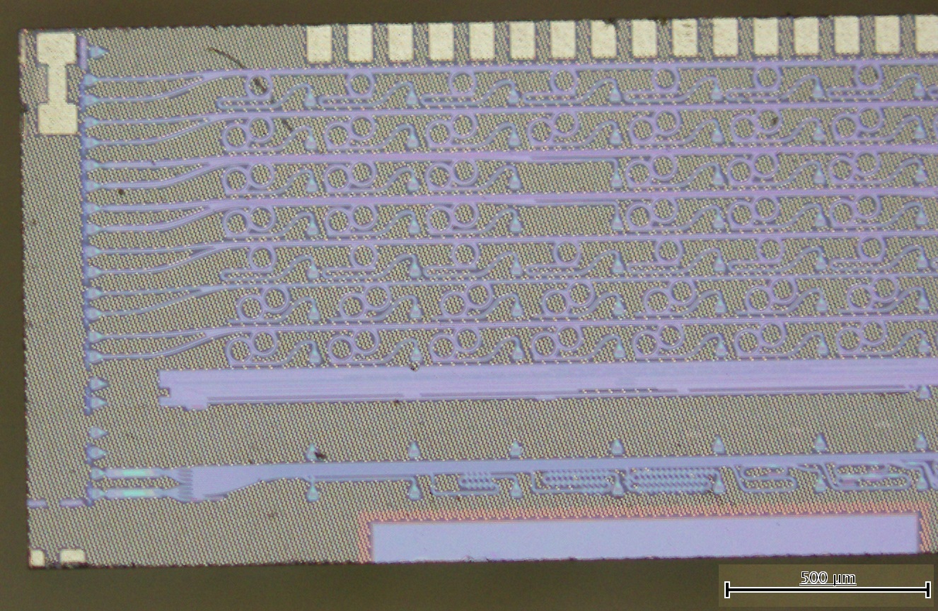
Silicon photonics technology addresses the need for higher data transmission bandwidth for long and short range communication systems. It is also identified as the promising technology for implementing (1) artificial neural network due its inherent parallelism and energy efficiency, (2) quantum computing with the prospect photon entanglement. Silicon being a high refractive index material, in combination with its native oxide allows one to produce submicron single mode waveguides for highly compact optical routing. Recently, there have been various photonics components developed independently on silicon photonics platform with exceptionally compact device
footprint and performance figures. Though standalone silicon photonic components provide extremely good device
response, system level integration needs to be further improved many folds to exploit the maximum capability of
silicon photonics. The major challenges being the temperature sensitivity of the silicon and the performance
degradation with respect to the fabrication error. As silicon is a high index material, even small fabrication variation
in the range of sub-nanometer could affect the performance of the resonant devices such as ring resonators. The
potential solution for the existing problems could be a multilayer substrate platform with various waveguiding layers
such as silicon and silicon nitride. In the multilayer platform, active and compact-passive devices are built on the
silicon layer. Whereas, passive devices which requires thermal stability and stringent fabrication requirements are
placed on silicon nitride layer. Thus, a stable system level integration can be achieved by utilizing multilayer
waveguiding platforms.