Dr. Mohamed Rezeq granted patent that may lead to a paradigm shift in the semiconductor industry.
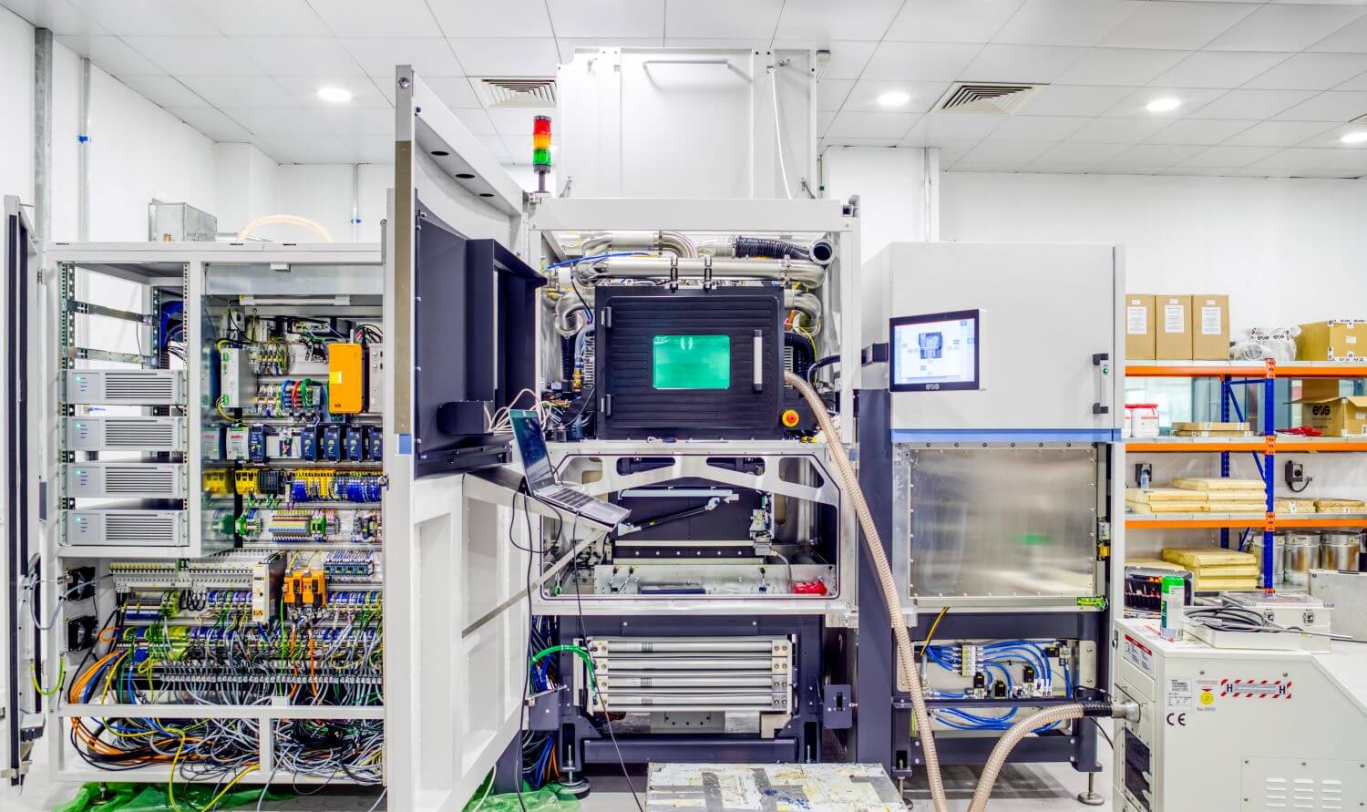
Abu Dhabi 15 January 2014: Khalifa University announced today that one of its faculty Dr. Mohamed Rezeq assistant professor of applied math and sciences has been granted a US patent for the creation of the world’s smallest semiconductor transistor. This new transistor is presumed to consume much less energy than existing technologies because it operates in a completely different way. This is because in the operation mode electrons jump (tunnel) directly from the nano metal particles the basic components of the transistor into the semiconductor with minimal loss of energy.
 Transistors are generally used to amplify and switchelectronic signals and electrical power and they are the fundamental building blocks of modern electronic devices and are present in all modern electronic systems.
“Dr. Rezeq’s work will very likely lead to a paradigm shift in the semiconductor industry and in particular in transistor design with a huge potential to build electronic devices that are more than 10 times smaller and consume much less power than any of the latest known technologies ” said Dr. Mohammed Al Mualla Senior Vice President for Research and Development at Khalifa University. “We are very proud of Dr. Rezeq for his accomplishments and we think that it is a testament to the culture of innovation that we try to foster at Khalifa University. We encourage all our faculty to conduct research activities at the highest level and to involve our students in their advanced research. In this way we are helping to build the knowledge economy envisioned in Abu Dhabi’s 2030 Vision.”
“I couldn’t have done it without the help and support given to me by Khalifa University especially their internal research fund ” says Dr. Rezeq “I couldn’t have done this within the relatively short time I had without the help of my Masters Student Ahmed Ali. Not to mention all the support from my colleagues and students which I am very grateful for.”
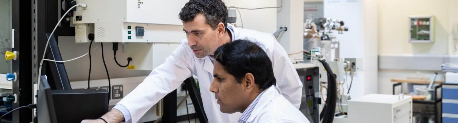
Nano-tips can be applied to many aspects of nanotechnology. For instance scanning electron microscope (SEM) and transmission electron microscope (TEM) use them as a source of electron beams. The smaller the size of the probe the higher the density of the electron beams which results in a significant improvement in the resolution and image brightness of such powerful microscopes so that more details can be observed. Nano-tips can also be used to look at biological molecules like DNA and nano materials in scanning probe microscopes like atomic force microscope (AFM) where a sharper tip means more information can be gathered.