
The new ‘nano-memory’ cell is designed as a type of non-volatile memory that can complete ‘read-write’ operations with a significantly smaller footprint and simple design using a single gold nanoparticle
To meet the growing demand for faster, smaller and more powerful electronics, a team of researchers from Khalifa University has developed a new type of ultra-small memory cell that could provide greater memory storage and improved processing speed on extremely small computer chips.
The new ‘nano-memory’ cell is tiny – only one gold nanoparticle thick, or about one-one thousandth the size of a human hair – and is sandwiched between very thin layers of aluminum oxide. It has a unique and simple structure that allows data to be ‘written’ onto it and ‘read’ from it by charging and discharging a single nanoparticle. Its simple design makes it easy to fabricate, and in turn, easily scalable and commercially viable.
Lead author Dr. Moh’d Rezeq, Associate Professor of Physics, along with Dr. Irfan Saadat, Professor of Electrical Engineering and Computer Science, Dr. Ammar Nayfeh, Associate Professor of Electrical Engineering and Computer Science, and Postdoctoral Fellows Dr. Ayman Rezk and Dr. Yawar Abbas, describe the new memory cell in a paper published in June 2020 in the journal Applied Physics Letters.
Computer Memory and MOSFETs
Computers represent information in binary code, which is written as sequences of 0s and 1s, known as a binary digit, or ‘bit.’ The files and programs on our computers comprise millions of these bits, which are stored in the computer’s memory, and then executed by the computer’s central processing unit.
There are two types of memory systems in a computer: Non-volatile memory (NVM), which is memory that can retrieve stored information even when the power to a computer has been turned off, and volatile memory, which is memory that processes information only when the computer is running.
NVM systems like flash memory use floating gate metal-oxide semiconductor field effect transistors to store each bit in a specific memory cell as an electric charge.
Metal-oxide semiconductor field effect transistors, or MOSFETs, are the building blocks of modern day computers. The billions of transistors found in all electronics today to switch and amplify electric signals are designed as MOSFETs.
Floating gate MOSFETs are designed in a way that allow the charge, which would normally pass through in a typical MOSFET, to be trapped in the ‘floating gate’ part of the system. This trapped charge represents a stored bit.
Dr. Rezeq and his team from KU have proposed a new, simpler memory cell structure to replace the floating gate MOSFET architecture.
The KU Nano-Memory Cell Design
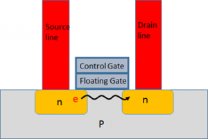
In a typical floating gate MOSFET, a stack of gates is arranged on a base, known as a substrate, that is made up of n- and p-type silicon semiconductors. The gates are insulated from the substrate by metal oxide insulating layers, also known as dielectrics. Source and drain terminals are connected directly to the substrate so that electrons can flow through a channel underneath the floating gate (see Figure A). The electrons don’t flow until a voltage is applied to the gate.
This structure, however, imposes some limitations on device performance and scaling, and also introduces some fabrication complexity.
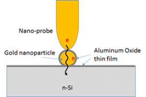
In Dr. Rezeq’s work the design is simpler. A single gold nanoparticle is placed on a silicon substrate that has been covered with a thin layer of aluminium oxide. Then, another thin layer of aluminium oxide is placed around the entire nanoparticle. In this design, the gold nanoparticle itself is the cell in which the charge is stored.
Their design does not involve the use of conventional source and drain terminals, and the substrate is only an n-type silicon semiconductor. Instead of source and drain terminals, they attach one electrode above the gold nanoparticle (see Figure B). In their proof-of-concept prototype, they used a nano-probe as the electrode.
After injecting an electrical charge (i.e. electrons) into the nanoparticle through the nano-probe, the researchers observed that a few electrons successfully tunnelled their way into the nanoparticle and became trapped in the nanoparticle itself. Thus, the team observed what would be called in a working computer as the ‘writing’ process.
To complete the ‘reading’ process, which is the process that takes place when the computer’s central processing unit executes and ‘reads’ from the memory cell, another voltage is applied through the electrode, allowing the CPU to read the current signal. If there is a charge in the nano-particle (which represents the ‘on’ state, or a 1 in binary code) the current signal will be less than the case when the nano-particle is discharged (which represents the ‘off’ state, or a 0 in binary code).
Dr. Rezeq credits the success of the nano-memory cell to the right size of the gold nanoparticle and the right thickness of the aluminum oxide layers.
“The selection of the nanoparticle size and the highly insulating – or high-K – aluminum oxide thickness is critical to optimize the tunnelling current and increase the charge retention time,” he said.
Metal oxides that are very good at insulating, including aluminium dioxide, are known as ‘high-k’ dielectrics. In floating gate MOSFETs, these insulating layers play a key role in ensuring the flow of electrons between the source and drain terminals does not affect the charge in the floating gate. In Dr. Rezeq’s nano-memory cell, the dielectric ensures that the charge stays trapped in the gold nanoparticle, and does not leak out. The dielectric has to be thin enough to let the charge in via the electron tunnelling process, but thick enough to keep it there when there is no voltage bias applied. Furthermore, their design allows erasing and writing memory data regularly.
“The nanoparticle itself here is used as a storage site of electrons but also regulates the current. Since the size of the nanoparticle can be controlled down to a few nanometers, this can result in a significant improvement in the capacity of the memory storage devices,” explained Dr. Rezeq. “Such devices are particularly interesting for their endurance, small operating voltage, and faster write/read cycles. These improvements are related to unique characteristics from the nanoparticles, particularly when combined with very thin high-k dielectrics.”
It is well accepted that nanotechnology will play a vital role in the ability to increase computing device performance across a broad range of applications and this work demonstrates where the future lies.
Dr. Rezeq plans to continue working on his nano-memory cell proof-of-concept and bring it into the next phase of development.
Jade Sterling, Science Writer and Erica Solomon, Publication Senior Specialist
30 September 2020