High-speed information to run your factory, produce energy efficiently, maintain safe infrastructure and monitor your vital health signs are just a few examples of how sensors can be used in industries such as biomedicine, manufacturing, renewable energy and aerospace.
The smaller and cheaper these devices can be made, the easier it is to incorporate sensors throughout the structure of your building (or factory), distribution network, environmental resources and phone.
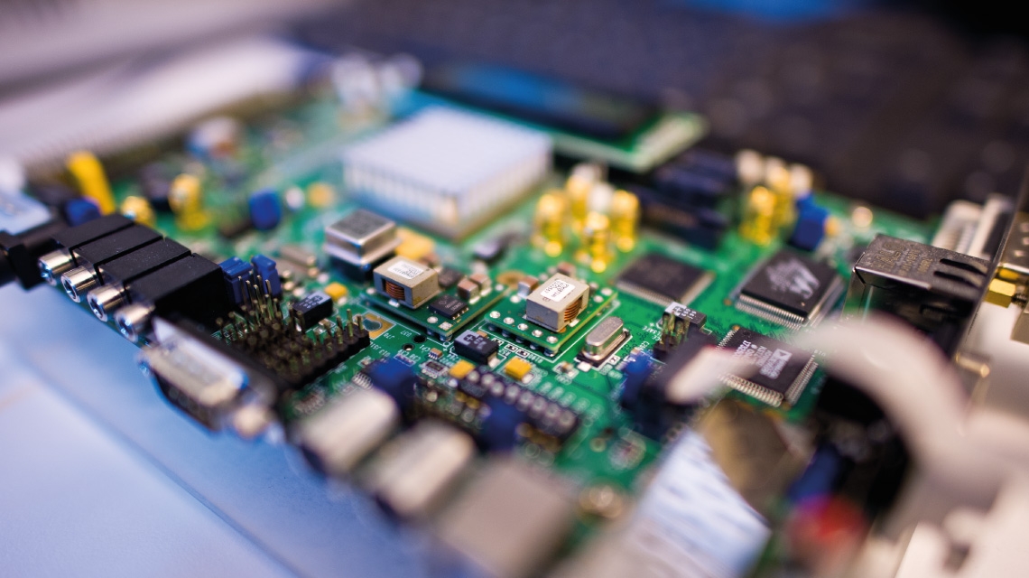
We are part of a team of Masdar Institute researchers looking to achieve that in an affordable and flexible manner by advancing sensors based on optical microelectromechanical systems, commonly known as optical MEMS.
MEMS are high-speed, low-powered, sand-sized machines. They can be found in your pocket (motion sensors in your smartphone), in your car (to trigger airbags), and in your inkjet printers (microfluidic ink valve).
Some of them – optical MEMS – react to light, with uses such as the mini projector common in most cinemas today. In addition to display technology, optical MEMS could be used for high-speed, high-resolution sensing, since slight changes in the properties of light can be correlated with subtle changes in material strain, temperature, and gas composition.
How do you decrease the cost and size while increasing the capability of optical MEMS sensors? The answer is to integrate on the same chip with photonic circuits.
Photonic circuits are a collection of microscale devices that detect, interact with and manipulate light. We are exploring a promising new platform for building and standardizing these sensors called the silicon-on-insulator (SOI) platform.
Several of our students at the Nano-Optics and Optoelectronics Research (Noor) Laboratory at Masdar Institute have already designed a few photonic circuits using such a material platform.
The appeal behind using SOI technology is that it is well suited and thus used by industry for all three types of microsystems: photonic, MEMS and electronic circuits.
Therefore you can potentially build all three types of devices on the same physical layer, opening the possibility for a whole new level of sensor functionalities and performances.
However, most foundry processes are optimized solely for a single type of microsystem.
The Noor team is working with two research entities in Singapore – GlobalFoundries Singapore and the Institute of Microelectronics (IME) – to develop a set of new sensors using the IME SOI opto-mechanical foundry platform, integrating MEMS and photonic devices.
Our team is mainly working on the photonics design, modelling and optical validation.
This collaborative research leverages complementary know-how from Masdar Institute and IME, with overall guidance from GlobalFoundries, to push the cutting-edge development of MEMS and enhance Abu Dhabi’s leadership in this burgeoning industry, which is expected to play a significant role in the UAE’s knowledge economy in the future.
Dr. Marcus Dahlem, Dr. Anatol Khilo and Dr. Clara Dimas are assistant professors of microsystems engineering at the Masdar Institute of Science and Technology and are members of the Nano-Optics and Optoelectronics Research Laboratory. This op-ed is the third in a series covering the research work under way at the Masdar Institute in the area of micro-electromechanical systems.