A recent paper presenting a breakthrough in the field of nano photo-detection and digital imaging has been published in Scientific Reports by Dr. Mohamed Rezeq, Associate Professor of Physics, and his research team at KU, Dr. Yawar Abbas, Dr. Ayman Rezk, Dr. Irfan Saadat, and Dr. Ammar Nayfeh.
The paper details a new structure and mechanism for nano photosensors that are very sensitive to light, extremely small in size, and with resolution capabilities below 10 nanometers – a much higher resolution than current photodetectors.
Photodetectors are sensors of light or other electromagnetic radiation that convert light photons into current. They are vital for fiber optic communication systems, process control, environmental sensing, safety and security, and various other scientific applications. Photodetectors are produced from semiconductor materials such as silicon and are most widely used in detecting light in the infrared region. The incoming light generates free electrons from the semiconductor material that it strikes to produce an electrical current. Due to this process, the current produced by the detector material changes as a function of the intensity of the incident light.
In current photodetectors, the photovoltaic effect, which produces the free electrons, is used to acquire image information with the phenomenon taking place at the p-n junction in the semiconductor, or the area where the positively and negatively doped layers of the semiconductor meet. The photovoltaic effect takes place when light with enough energy strikes this junction to produce the separation of charge, resulting in a voltage that encodes the image information.
Photodetectors are continually seeing improvements in performance, cost, and speed, with nanostructured materials very promising for performance improvements. To produce a smaller, scaled-down semiconducting device, with lower power consumption, investigating photodetection at the nanoscale metal-semiconductor interface is essential.
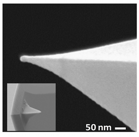
Dr. Rezeq’s paper investigates a new structure of photo- detectors based on nano metal-semiconductor junctions, referred to as nano-Schottky junctions, using gold-coated conductive atomic force microscope nano-probes and an n-doped silicon substrate. These metal nano-probes can be readily replaced by metal (like gold) nanoparticles deposited on Si substrates for fabricating the actual nano-photo sensors.
“The fundamental operation of the photodetector depends on the transition of the electron from the metal nanoparticle upon the absorption of the photon (light) energy,” explained Dr. Rezeq. “This process, in turn, manifests as an increase in the magnitude of electric current during the electrical measurements of these devices.”
The material used to make a photodiode is critical to defining its properties, because only photons with sufficient energy to excite electrons across the material’s bandgap will produce significant photocurrents. Bulk Semiconductor photo defectors like Silicon and germanium have an important limitation in that they are not suitable for operation with photons that have energy less than the bandgap energy. Nanostructured materials can have a huge impact if they can widen the reach of silicon and germanium across the wavelength spectrum while maintaining the other long-standing advantages of these materials.
“This is a new structure and mechanism for fabricating nano-photo sensors that are very sensitive to light and extremely small in size,” explained Dr. Rezeq. “This is because the basic structure of these photo sensors is made of metal nanoparticles that are in the range of 5-20 nm, also called plasmonic nanoparticles, and placed on a silicon substrate. Because of their small size, the electrons can move freely within the nanoparticle and become very sensitive to light.”
“When the light hits such nanoparticles, even with very little energy, electrons can easily jump or tunnel through a very thin barrier to the silicon material which results in a photoelectric signal,” explained Dr. Rezeq. “Because these nanoparticles don’t have a specific energy band gap like current photo-sensors, this makes them very sensitive to any light wavelength ranging from very low energy infrared to high energy ultraviolet.”
“The optoelectronic characteristics of nanostructures such as nanowires, quantum dots and nanosheets reveal the fascinating features of nanomaterials,” said Dr. Rezeq. “Owing to their excellent response to the light, in terms of dynamic range and sensitivity, these nanostructures placed themselves as outstanding candidates for the building blocks of a new generation of photodetectors.
 In this paper, Dr. Rezeq and his team demonstrated the effect of light irradiation on the tunneling current of gold nano-probes and nano-silicon interfaces using conductive-probe atomic force microscopy (C-AFM).
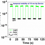
C-AFM is used as a powerful tool to investigate photodetection at nano-scale metal-semiconductor junctions. A conductive nano-tip (nano-probe) is scanned in contact with the sample surface, while a voltage is applied between the tip and the sample, generating a current image. By systematically approaching the nano-tip to the surface of the substrate, prominent differences of tunneling current magnitude under dark and light conditions were observed. The research team noted that the tunneling current and the sensitivity of photodetection was higher for tips of smaller radii, which they attributed to the higher field intensity generated by the smaller tip radius, reducing the barrier width of the interface.
“The main advantage of C-AFM electrical measurement is its ability to gather local conductivity information,” said Dr. Rezeq. “Due to the very small size of the nano-tip, one can detect the effect of light on the tunneling current from the nano-tip to substrate due to narrowing of the interface barrier width by the enhancement of local electric field at the nano-tip-substrate interface.
“Studies have revealed that for nanoscale Schottky diodes, the Schottky barrier width and hence the diode performance becomes a function of the diode size,” explained Dr. Rezeq. “Consequently, the contribution of the tunneling current to the total conductance is greatly enhanced. The gold nano-tips and the CAFM measurements further showed that the size of nano-Schottky contacts at nanoscale prominently affects the behavior of semiconductor devices.”
According to the research team, this research will pave the way for a new direction in the field of ultra-sensitive photodetectors focusing on photoresponse-induced tunneling current in nano-scale Schottky junctions.
Jade Sterling
News and Features Writer
31 October 2019