The 19th-century builders of bridges, skyscrapers, metropolitan railroad stations, and deep-water harbors had no supercomputers, desktops, laptops, or tablets.
Instead, they had armies of draftsmen whose sole function was to produce the blueprints, layouts and elevations that field engineers and construction workers would later transform into a bridge, a tower, or a dam.
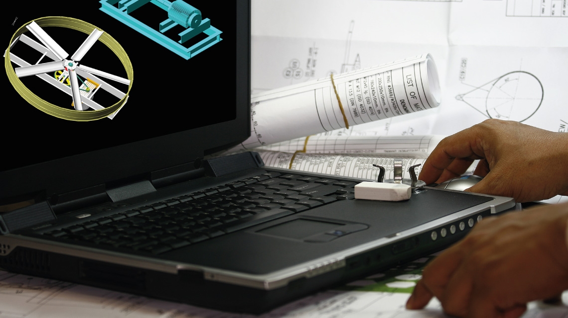
The advent of the computer has changed all this. It has become the drawing board, and the designers – be they architects, engineers, or inventors – have acquired new skills and become their own draftsmen.
This transformation has resulted in a new field of engineering called Computer-Aided Design (CAD), turning the computer into a virtual machine shop or workbench where the engineer can iterate between concept and construction until all design specifications are satisfied.
More important than aiding design, CAD facilitates re-design and therefore opens up the creative field and presents engineers with possibilities that were never before possible.
CAD is not just about large-scale structures. It is also about our micro-scale designs, our micro-electronic chips, micro-sensors, and microelectromechanical systems (MEMS).
With CAD, we can use computers to design better computers and microchips to design more complex, faster microchips. CAD doesn’t just help us design structures, it allows us to analyze how they will behave.
While the drafting table and its blueprints are spatial constructs, the computer and its graphics interface are both spatial and temporal. Objects can be visualized in space, and their behavior over time examined.
This latter aspect is what engineers call simulation, and it is crucial in gaining a deeper understanding of the dynamics of the design in responding to external forces or internal changes.
This aspect is particularly important in the simulation of MEMS, which often encompass more than one physical domain, thus making the analysis and verification of their behavior quite challenging.
While CAD for electronics has just to deal with flows of electrons through electrical components and electronic devices, CAD for MEMS has to also deal with masses, velocities, and accelerations.
It has to deal with both the mechanical domain and the electronic domain. With some of the more complex MEMS sensors, it has also to deal with the fluidic, thermal, and optical domains.
MEMS CAD has to run complex three-dimensional computer simulations, not unlike the simulations that civil engineers conduct for bridges and high-rise buildings or the simulations that aerospace engineers run for aircraft fuselage, wings, and engines.
To help advance MEMS CAD so that it is able to continue to serve as an enabling tool for innovation in engineering and design, the Masdar Institute is focusing the attention of its Institute Centre for Microsystems (iMicro) addressing some of the most important challenges in MEMS design and simulation and on developing student skills and mastery of cutting-edge MEMS CAD tools. The research and training at Masdar Institute are being conducted under its TwinLab framework with Singapore’s A*STAR Institute of Microelectronics. The strength of Masdar Institute’s CAD research is that it closely parallels the MEMS devices currently under design within TwinLab, including MEMS for motion sensing, energy harvesting, ultrasound sensing, optical sensing and computer-aided design for MEMS devices.
Through this partnership funded by Mubadala Technology, GlobalFoundries and the Singapore Economic Development Board (EDB), Masdar Institute is both acquiring and contributing to the technical expertise required to develop the advanced MEMS CAD tools of tomorrow.
Dr. Ibrahim (Abe) Elfadel is professor of electrical engineering and computer science and head of the Institute Centre for Microsystems (iMicro) at the Masdar Institute. This op-ed is the second in a series of op-eds covering the research work being conducted at the Masdar Institute in the area of MEMS.