KU Researchers Grow Vertically Aligned Graphene Nanosheets at Low-Temperature and Explore Potential Application as Biosensor in Lab-On-Chip Technology
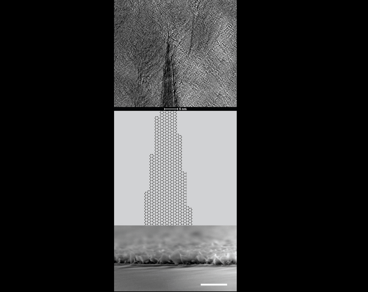
The world’s tallest building – the iconic Burj Khalifa – has been reconstructed at the nanoscale entirely out of structured graphene at Khalifa University’s Laboratory for Energy and Nano Science (LENS).
The new ultra-small Burj Khalifa-inspired graphene structure (which measures just 100 nanometers in height) has potential application as an electrochemical sensor in a “lab-on-a-chip” device for medical diagnostics and drug development, says Dr. Matteo Chiesa, Professor of Mechanical Engineering at KU and head of LENS.
The unique 3D structure was grown at a low temperature of 625°C. Traditionally, graphene is grown at about 1000 °C. The new process offers a more sustainable and scalable approach to producing the ultrathin electronic material on different substrates.
Graphene is considered a ‘wonder material’ since it was first discovered in 2004. It has the highest known thermal and electrical conductivity, and is stronger than steel, extremely lightweight, and flexible. Despite its outstanding mechanical, thermal and electrical properties, as an ultrathin 2D material, it is difficult to translate graphene’s 2D strength into useful 3D materials, which could then be more easily used in devices, buildings and vehicles.
3D graphene structures address this challenge by leveraging graphene’s unique properties in a 3D form with its own unique properties.
Vertically aligned graphene nanosheets is one such 3D graphene structure that has excellent electron transport properties, outstanding mechanical strength, high chemical stability, and enhanced electrochemical activity. They are 3D networks of carbon nanomaterial that grow in rows of vertical sheets – graphene nanosheets – providing a large surface area for greater charge storage capacity.
The KU team has successfully grown vertically aligned graphene nanosheets on pieces of germanium, a type of semiconducting material, for the first time.
“No one has attempted to grow graphene nanosheets on germanium before, only on semiconducting materials like silicon, which require a higher temperature,” explained Dr. Chiesa.
“We used a plasma enhanced chemical vapor deposition process to grow the vertically aligned graphene nanosheet arrays. The 3D graphene structure we developed has a strong contact with the germanium substrate, exposed edges, and easily accessible surfaces,” said Dr. Amal Al Ghaferi, Associate Professor of Mechanical Engineering. “These features give it a large surface area and excellent electron transfer capability, which make it an excellent candidate as an electrode material for energy storage applications or lab-on-chip devices.”
A paper describing the new research was recently published in the journal Carbon. Authors include Dr. Al Ghaferi, Dr. Chiesa, PhD student Mariam Al Almahri. MSc student Abdulrahman Al-Hagri, and six others.
While graphene is typically grown through a process known as chemical vapor deposition (CVD), plasma-enhanced CVD uses microwaves to turn gases in a chamber into a reactive plasma, which makes it possible to grow graphene at lower temperatures.
“In order to have pure carbon flow for the building of graphene, we need to ‘take out’ the hydrogen molecule from the methane; a process which requires significant energy. This can be done at high temperatures, or by means of plasma bombardment of the methane molecules, which we did through the plasma enhanced CVD,” Dr. Chiesa explained.

The uniquely designed graphene nanosheets not only resemble the Burj Khalifa at a significantly smaller scale, but produce an enhanced electric field at the structure’s tip. It is this feature that makes the 3D graphene structure particularly useful for lab-on-chip applications.
A lab-on-a-chip is a biosensor device the size of a USB flash drive, where small quantities of fluids or cells are manipulated through very small channels in order to synthesize and analyze chemicals at a very miniaturized scale. Lab-on-chip technology is useful for analyzing cells, diagnosing diseases, and testing new drugs. It uses nanosensors to detect very low concentrations of a particular chemical or biomarker, which are proteins, DNA molecules, or other measurable indicators that show the presence of a disease.
The tip of the KU 3D graphene structure works like an antenna. When a highly focused laser is directed at the graphene structure, the enhanced electric field at the tip is observed. The enhanced electric field, in turn, means it can be used as a nanosensor to detect biomarkers in lab-on-chip systems with a higher degree of sensitivity.
“We can configure an infrared waveguide with the graphene structure so that we can be very sensitive to the presence of certain biomarkers. Usually this require a discrete type of blood sampling every several hours. With the enhanced sensitivity achieved here, however, we can monitor the patient continuously,” Dr. Chiesa said.
Erica Solomon
Senior Editor
28 October 2019